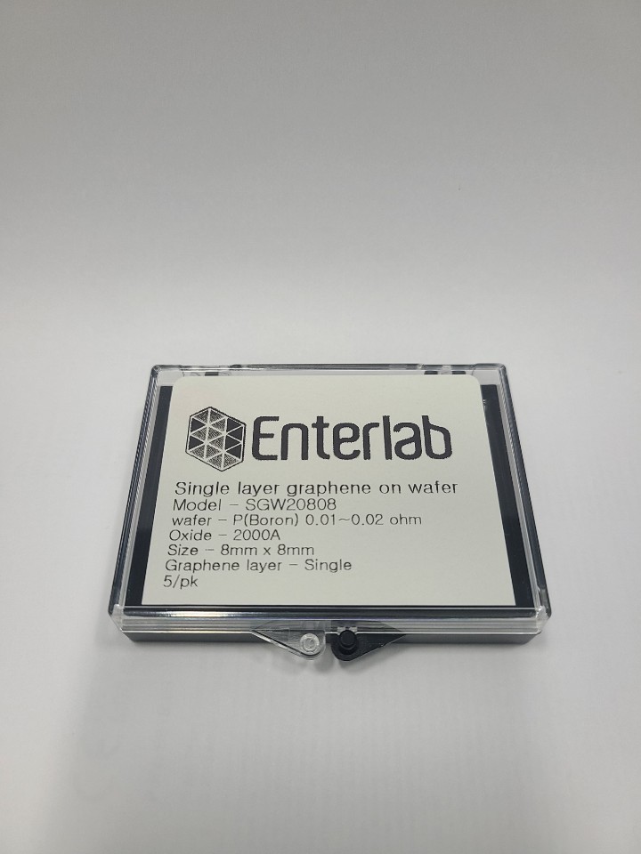
Single layer graphene on wafer

Silicon wafer
■ Graphene layer - single
■ Wafer - P(Boron) 0.01~0.02 ohm
■ Oxide - 2000A
Quartz wafer
■ Material : Fused Silicia
■ Grade : UV Grade
■ TTV (Total Thickness Variation) : ± 10㎕
■ RA (10Å), Double Side Polishing
Glass wafer
■ PYREX® Glass
■ TTV (Total Thickness Variation) : ± 10㎕
■ Bow (± 30㎕), RA(15Å)
■ Double Side Polishing (DSP)


